Whether you are designing life-saving devices or industrial equipment, Printed Circuit Board Assemblies (PCBAs) are a necessity. PCBA designs are becoming increasingly complex, and yet, are required to fit in smaller and smaller spaces.

You may also be tasked with redesigning layouts due to obsolescence or the unavailability of existing components as a result of global supply chain issues. Regardless of the cause dictating the requirements, PCBA prototyping is often a needed first step to create a functional product designed for manufacturability.
Whether you’re a skilled designer or just starting, there are some PCBA prototyping factors to consider. From creating functional designs to making sure it flows efficiently during production, this article looks at common issues to keep in mind when designing, building, and testing PCBA prototypes.

Why Do You Need PCBA Prototyping?
It’s critical to confirm a PCBA design is sound before starting a full production run. Regardless of how meticulously designers work on a project, there can be errors. Any miscalculations, and a lack of understanding of the manufacturing process can jeopardize the outcome. If these issues are not identified before production, it can result in costly delays, shutdowns, wasted materials, and labor-intensive iterative redesigns.
Investing in PCBA prototyping that takes into account good design practices, testing requirements, and DFM (design for manufacturability) design processes can ensure a smooth design transfer to production.
What Are the Common PCBA Prototyping Issues?
Creating a quality, functional prototype is the first step to building a high-quality, high-performing final product. However, not identifying issues during each phase of development may complicate the prototyping process.
PCBA Design Issues
Higher-level design issues include not considering the form factor needed and current technology applications available. It’s critical to also understand the tradeoffs between the design elements, product performance, and cost.
The number of potential design flaws in just the PCB board layout is quite high and will also manifest in the DFM process. Some of the most common design flaws to avoid at the onset, include:
- Poor trace routings leading to acid traps
- Layouts that allow for plating voids
- Using very small components in large copper ground planes resulting in the tombstoning of components
- Creating too small of a footprint resulting in bad solder joints not giving a good heel
Prototype Build and Test Issues
PCBA prototyping aims to design, build, and test a production run of PCBAs. However, issues can arise with the building and testing of the prototype itself.
Creating a prototype design that’s incompatible with the board layout size, requires running jumper wires, or other workarounds. This can often lead to DFM issues later in the process.
Not allowing for test access to a point or node within a specific circuit makes testing very difficult. It can result in shorts, opens, or other failures making their way through design into the production phase.
Design For Manufacturability (DFM) Issues
Because there is often no direct contact between the designer and manufacturer during the design stage, it can lead to miscommunications. The design engineer may not realize until later that the layout doesn’t match the manufacturer’s requirements. This mismatch can cause project delays, lost revenue, low closure rates, extended lead time, and inadequate production capacity.
Typical DFM issues include:
- Calling out components and layouts that are different from the layout on the printed circuit boards. It results in design to BOM incompatibility.
- Calling out components that are not available due to supply chain complications.
- Configuration incompatibility where the individual parts are too big or small for the board layout.
- Work-arounds such as the jumper wires mentioned previously to accommodate component and layout incongruities. It will then put the functionality of the end product in doubt.
- Components placed too close together, making assembly challenging.
- Components placements that interfere with a mounted bracket or placement of the board into a housing.

What Are Some Solutions to Avoid These Issues?
PCBA makers servicing critical and non-critical sectors strive to reduce errors as much as possible. The only approach to ensuring high-quality PCBAs is to have a thorough awareness of typical mistakes and how to prevent them. If you don’t follow proper precautions, the end product’s performance will suffer. Here are a few techniques to avoid frequent PCBA prototyping problems.
Create Well-Defined Functional and Physical Requirements
The PCBA design phase needs to define clearly:
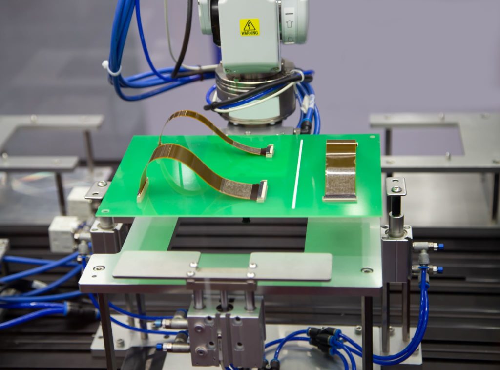
- The desired form factor – using a typical rigid FR4 fiberglass board or using a more flexible ribbon technology to navigate smaller spaces or complex geometries
- The number of layers – more functional complexity results in more signals which are usually handled by adding more layers, increasing the overall thickness of the board
- The optimal trade-off between performance and cost – defining the parameters for form, fit, and function that will provide the desired outcome while keeping the project within budget
PCBA design is a complex process involving careful consideration of every element and meticulous attention to the smallest details. Ignoring any detail can mean throwing away weeks of effort and the need to start over. Some examples include forgetting to account for a material factor or a functional necessity, making your existing design unusable.
The initial stage in any complicated process is usually the most important, and PCBA design is no exception. Working with an experienced engineering service provider, like Nortech Systems, helps you easily spot these potential downfalls. Discovering problems before the prototype is built will end up saving you time, money and frustration.
Create Well-Defined Test Requirements
To prevent the common PCBA prototyping issues, avoid the previous design layout flaws. The next step is to develop a well-thought-out set of testing requirements and design aspects that allow for that testing.
You may rapidly discover the most prevalent PCBA prototype issues using sound testing techniques and the appropriate equipment. Take the following test options into consideration:
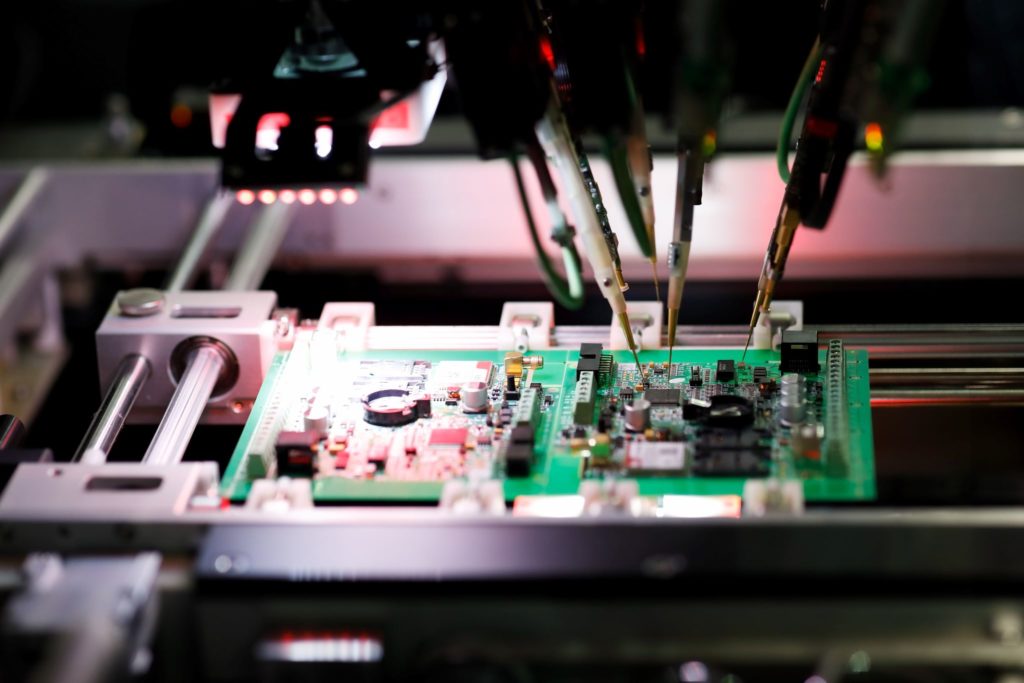
- A flying probe is the least expensive of all the testing methods and is used to test component placement and orientation.
- Automated test platforms are relatively more costly since they require a dedicated test fixture. However, the automated test platforms are faster than the flying probe method, taking between 30-60 seconds to test a PCBA board fully.
- Mid-range ATE tests combine functional and in-circuit testing. It aims to verify whether the PCBA powers up correctly, the circuitry functions as intended, and the final product meets specifications.
Maintain a PCBA Prototyping Issues Log
Avoiding DFM difficulties is better than allowing them to damage your PCBA during production and then searching for a solution. Designers must make good decisions for DFM to work, including fixing issues before they arise.
Maintaining a PCBA development issues log creates a connection between design and manufacturing. The result is a knowledge base that will enhance the outcome of your project while providing a better starting point for future projects.

Flexibility Is the Key
Everything from medical diagnostic equipment and treatment devices to oxygen and refueling systems in the aerospace and defense industries uses PCBAs. Their vast integration into every facet of life and business is why it’s vital to understand the causes of PCBA failures and how to avert them.
Find a reliable supplier who is flexible and conversant with the PCBA prototyping and manufacturing processes. This is the best way to guarantee that you’ll develop a PCBA of the highest quality. A manufacturer that implements and maintains DFM logs builds a partnership with you, design, and production.
Collaborate with Nortech Systems to develop your ideal prototype into a functioning, highly aesthetic, and perfected product ready for implementation.
Nortech has access to a wide array of PCBA design and manufacturing technologies. We are skilled at picking up your design, whether it’s on the back of the envelope, completely functional, or needing help with supply chain complications.
Together we will develop a high-quality, high-performance PCBA prototype to increase the success of your project.
Reach out to us at Nortech Systems today for reliable and experienced PCBA prototyping.

